The semiconductor industry's AI strategy is fragmenting along workload lines. AMD and Google both used this product cycle to split their offerings into purpose-built parts rather than pushing a single general-purpose design at every customer. The pattern across the stories logged on this beat is product-line segmentation: the recognition that AI infrastructure is no longer one job, and that a chip tuned for one kind of job is the wrong chip for another.
AMD Divides Its Server Line by Core Shape
The clearest expression of the trend is AMD's Epyc 6 series, also known as Venice, which the company introduced for AI agent workloads, as SiliconANGLE reported. AMD built 10 CPUs into two groups. One set carries a large number of relatively slow cores. The other carries fewer, higher-frequency cores. That is a deliberate design fork, not a modest refresh. Depending on the workload, the customer is steered toward a different physical shape of processor.
The logic behind such a split is legible from the descriptions. Workloads that reward parallelism benefit from many cores, even at lower clock speeds. Workloads that reward per-core responsiveness benefit from fewer, faster cores. AI agent workloads, which the Epyc 6 line explicitly targets, mix both kinds of demand, and AMD has chosen to address the mix with two product profiles instead of one compromise part. Buyers now face a more consequential configuration decision, and the vendor that guides that decision well gains an advantage.
Embedded Systems Get Their Own Branch
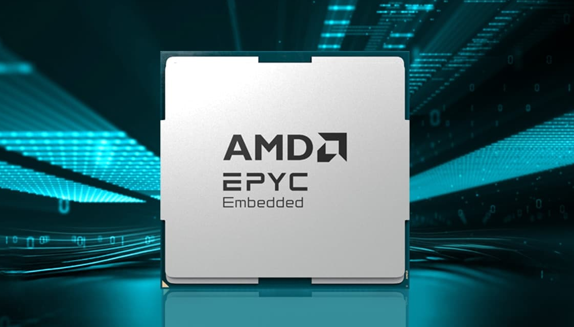
AMD pushed the same architecture in a different direction with its 6th Gen EPYC Embedded 9006 Series SP7 processors, which SiliconANGLE reported bring Zen 6 architecture to embedded systems. The stated targets are semiconductor automated test equipment, or ATE, and enterprise storage systems. These are not data-center training clusters. They are specialized machines with different constraints: validation environments, test floors, and storage controllers where the processor must fit a fixed system design and run reliably for long stretches.
That the same core architecture now reaches embedded ATE and storage hardware is the second half of the pattern. AMD is not merely splitting one server line; it is extending the Zen 6 family across deployment contexts that used to sit outside the mainstream server conversation. For US semiconductor manufacturing and test operations, the practical effect is that the compute layer underlying chip validation can advance on a faster cadence. Test equipment has long been a quiet bottleneck in the chip supply chain, and positioning current-generation server silicon inside it matters to the companies running those lines.
Google Splits by Function, Not Just by Generation
Google's contribution to the pattern is a pair of new tensor processing units that broaden its chip portfolio to more use cases, as TechCrunch reported. The two capabilities named are confidential model training and more memory capacity. Those are not interchangeable requirements. Confidential training implies isolation guarantees around sensitive model data during the training process itself. Greater memory capacity addresses the size of models and working sets that must be held close to compute.
By building two specialized chips rather than folding both traits into one design, Google is making the same bet as AMD: that the cost of a general-purpose part which does everything adequately exceeds the cost of separate parts that each do one thing well. That is a meaningful shift for the largest buyers of AI hardware, because it makes the composition of a training cluster an exercise in matching chip to task rather than standardizing on a single accelerator SKU.