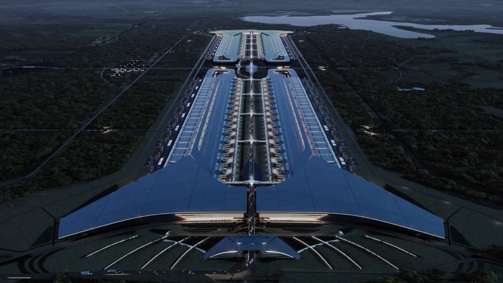
Elon Musk’s Terafab is aiming to reach one million wafers a month after 2032, with a memory output target of roughly 700,000 wafers, according to details reported by The Elec and Jiji Press. The figures put the project’s planned memory capacity in the same range as established memory producers, though the comparison comes with caveats. Terafab’s 700,000 figure covers all of its expected memory output, which could be NAND or DRAM, while estimates for Samsung and SK hynix count DRAM only.
Samsung’s DRAM capacity was estimated last year at 650,000 to 700,000 wafers a month, and SK hynix is reportedly at about 550,000, with about one million as a goal by 2030. Measured on that basis, Terafab’s memory portion alone would be 3.5 times the reported 200,000 at SK hynix’s Wuxi fab in China. Industry observers were skeptical when Musk announced the plans in March, but orders are now leading more companies to view the effort as a real business opportunity.
The schedule is aggressive by industry standards, since moving from planning to volume production at a leading-edge fab typically takes three years or more. Terafab is targeting volume production in the second half of 2028. Procurement officials from the company reportedly visited Japan earlier this month to meet local suppliers and work out details for bringing in equipment, with some suppliers asked to deliver within a few months.
Terafab representatives also visited the booths of about 10 Korean materials, parts and equipment firms at SEMICON West, and some NDAs were signed. On the logic side, Jiji Press reports Terafab is working with Intel to adopt its 2nm and 1.4nm processes. The memory side is less defined: technical help from a Taiwanese company is under consideration, but no partner has been named, leaving 70% of the planned wafers without a disclosed process technology.
A Tesla job listing for a Terafab Memory Process Integration Engineer, reported in August, covers end-to-end DRAM process integration and DRAM node development and supports emerging memories such as MRAM, RRAM and 3D DRAM. Terafab has not said how its DRAM would be divided among products such as HBM and LPDDR, both mentioned in its job postings, or whether it will make and stack the DRAM itself or package chips it brings in.
Building a cutting-edge logic fab on U.S. soil is its own challenge, and Tesla and SpaceX lack chip-manufacturing experience. Musk, on a SpaceX call last month, called Terafab’s dates very aggressive and said he put big error bars on the timeline. The first SRAM test chip is targeted for around May or June 2027 at the Austin research facility.
How TSMC might fit in remains open. TSMC says any fab with its involvement has to be run by TSMC, while Musk said his own companies would build and operate Terafab, a scenario that could leave TSMC as a space tenant. The spending plans are known: $16.8 billion for the first phase in Grimes County, Texas, with total investment of up to $119 billion if later phases proceed. A pilot plant could be completed as early as July 2027.
More hardware news from TechManNews.